
Integrated Circuits of Patterning Aluminum by Plasma Etching and Patterning of Copper by Damascene Plating
Question
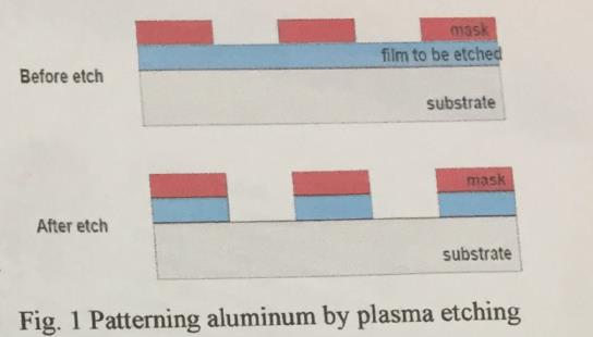
Very- large-scale integration (VLSI) of integrated circuits (ICs) is the combination of thousands of transistors on a single piece of silicon wafer. Metallic interconnects from one transistor to another on the silicon wafer make VLSI possible. Plasma etching is a process in which the plasma (a relative ion beam) generates volatile etch products on unmasked blue material (see figure 1). Here the blue material can be sputter deposited aluminum but not copper because copper dose not from volatile species with a plasma (cannot be etched this way). Plated copper is desired instead of sputter deposited aluminum because the copper is a better electronic conductor than the aluminum. Using a copper instead of aluminum interconnect results in an equivalent but smaller IC because there is less resistive heating with the copper.
Copper patterning is done by Damascene plating (see Fig. 2) in which the underlying silicon layer is patterned by plasma etching forming open trenches in the silicon where a thick coating of copper is plated and overfills the trenches on the silicon. The overfill is removed by chemical-mechanical planarization (CMP) leaving an electronically conducting copper line inside the silicon which can act as an interconnect.
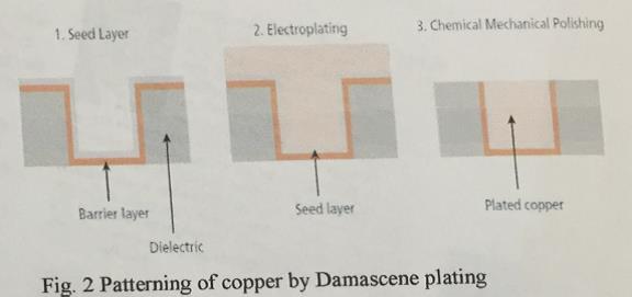
Which figure shows metal inlaying?
- Figure 1
- Figure 2
- Both figure 1 and figure 2
- Neither figure 1 or Figure 2
Summary
This question belongs to physics and discusses about integrated circuits of patterning aluminum by plasma etching and patterning of copper by damascene plating.
Total word count: 96